Advantages and disadvantages of PCB antennas
Introduction
Printed Circuit Board (PCB) antennas are becoming increasingly popular due to their ability to provide a low-profile, cost-effective and high-performance solution for wireless communication systems. The design of the antenna on a PCB is critical to achieve optimum performance when using the antenna for transmitting or receiving signals. In this paper, we will discuss the advantages and disadvantages of PCB antennas and the various techniques used to design PCB antennas. In addition, we will delve into the design of the antenna, the layout of the PCB and the selection of materials to achieve optimal performance.
Advantages and Disadvantages of PCB Antennas
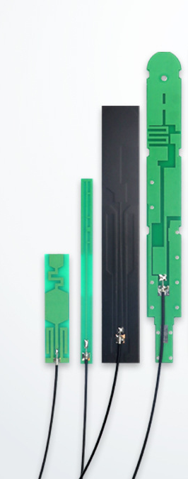
PCB antennas have many advantages over traditional wire antennas, including low cost, low profile, ease of installation and a shorter design cycle. The use of PCB antennas can result in a more efficient and reliable wireless communication system. However, there are also some disadvantages associated with the use of PCB antennas. One of the most significant disadvantages is the limited bandwidth available in a PCB antenna. The bandwidth is determined by the physical dimensions of the antenna and the wavelength of the signal. PCB antennas are also susceptible to interference from other components in the circuit.
Techniques for Designing PCB Antennas
There are several techniques that can be used to design a PCB antenna. The most common techniques include microstrip patch antennas, inverted-F antennas, and chip antennas. Microstrip patch antennas are used when high gain and directional radiation patterns are required. These antennas are typically small in size and can be easily integrated onto the PCB. Inverted-F antennas are used when a broadband solution is required. These antennas are also small in size and can be integrated onto the PCB. Chip antennas are used when a low-cost and small-sized implementation is required. These antennas are typically mounted on the surface of the PCB and require minimal space.
Design of the Antenna
The design of the PCB antenna is critical to achieve optimal performance. The design should take into consideration the operating frequency, the antenna's gain, the radiation pattern and the impedance matching. The operating frequency is determined by the application and the communication system. The gain of the antenna is critical to ensure that the signal is transmitted and received with sufficient power. The radiation pattern of the antenna defines the direction in which the signal is transmitted or received. Finally, the impedance matching is critical to ensure that the antenna can transmit and receive signals with minimal loss.
Layout of the PCB
The layout of the PCB is also critical to achieve optimal performance from the PCB antenna. The PCB should be designed to minimize the noise and interference generated by other components in the circuit. The design should also take into consideration the ground plane, which can be used to improve the performance of the antenna. The ground plane provides a low impedance path for the antenna to operate. Furthermore, the ground plane can help to reduce the effects of coupling and radiation from other components in the circuit.
Selection of Materials
The selection of materials used in the PCB is critical to achieve optimal performance of the PCB antenna. The substrate material used in the PCB should be carefully selected to ensure a low-loss transmission line. The substrate material should also be selected to match the dielectric constant of the antenna to ensure that signal reflections are minimized. Furthermore, the substrate should be designed to have a low loss tangent to minimize the losses incurred by the antenna.
Conclusion
In conclusion, the use of PCB antennas has many advantages and disadvantages. The design of the antenna, layout of the PCB and selection of materials can significantly impact the performance of the antenna. The use of microstrip patch antennas, inverted-F antennas, and chip antennas is common techniques used to design PCB antennas. The design of the antenna should take into consideration the operating frequency, the antenna's gain, the radiation pattern and the impedance matching. The layout of the PCB should minimize noise and interference while providing a low impedance path for the antenna. Finally, the selection of materials used in the PCB should ensure a low-loss transmission line and should match the dielectric constant of the antenna to minimize signal reflections.
