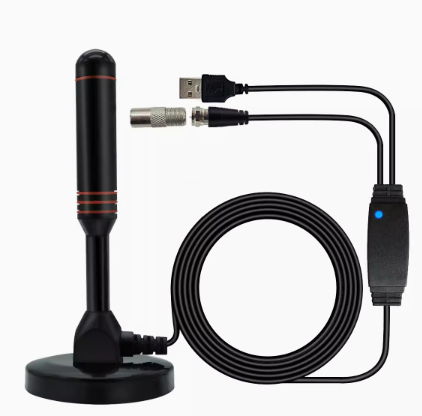
PCB antenna wiring steps
A PCB antenna is an essential component of many types of electronic devices that rely on wireless communication capabilities. When designing a PCB antenna, one of the most critical aspects to consider is the routing of the antenna traces. In this article, we will guide you through the process of routing your PCB antenna successfully.
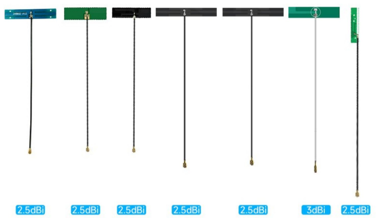
1. Determine the Antenna Type:
The first step when routing a PCB antenna is to determine the type of antenna you want to use. There are various forms of antennas such as monopoles, dipoles, patch antennas, helical antennas, etc. Each of these antennas has certain advantages and disadvantages, and the selection mainly depends on factors such as frequency range, gain, polarization, radiation pattern, and form factor. Make sure to have a clear understanding of the design requirements and select the appropriate antenna type for your application.
2. Location:
The location of the antenna is also a crucial factor to consider during the routing process. The antenna's placement should be in areas with low electromagnetic interference (EMI) and away from other high-frequency components like microcontrollers, RF transceivers, filters, etc.
3. PCB Materials:
The choice of PCB material can affect the performance of your antenna. Low-loss materials such as Rogers or FR4 high Tg can result in better efficiency and reduce signal losses. Make sure to check the datasheet of the PCB material to ensure the dielectric constant, thickness, and substrate properties are compatible with your antenna design.
4. Trace Routing:
Routing the antenna traces can be a challenging task, and it requires careful attention to detail. Several guidelines should be followed to ensure the antenna performs optimally:
- Antenna trace length should match the calculated wavelength of the operating frequency. If the traces are too long or too short, they can result in resonance problems and affect the impedance matching.
- The traces should be wider to reduce resistance and minimize signal loss.
- The traces should be kept as straight as possible to prevent unwanted coupling and radiation patterns.
- The traces should be kept away from signal lines carrying high-frequency signals to avoid signal cross-talk.
- Traces that are close together should be separated by a ground plane to minimize coupling.
5. Ground Plane:
The ground plane is essential for the antenna's performance and can improve signal integrity by reducing EMI and electromagnetic radiation (EMR). Ideally, the ground plane should be a flat and continuous plane that covers the entire board's bottom layer. Ensure there are no cutouts, gaps or slots on the ground plane to avoid reflection and interference.
6. Testing:
Testing is a critical aspect of antenna design and optimization. Use test equipment such as a spectrum analyzer or a vector network analyzer to measure the antenna's impedance, radiation pattern, gain, radiation efficiency, and so on.
In conclusion, routing a PCB antenna requires careful planning and attention to detail. The correct selection of antenna type, location, and routing, along with an adequate ground plane and testing, can result in optimal performance. Remember to simulate your design using software tools before manufacturing to prevent any unexpected issues.
